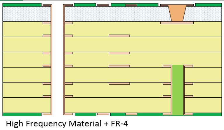
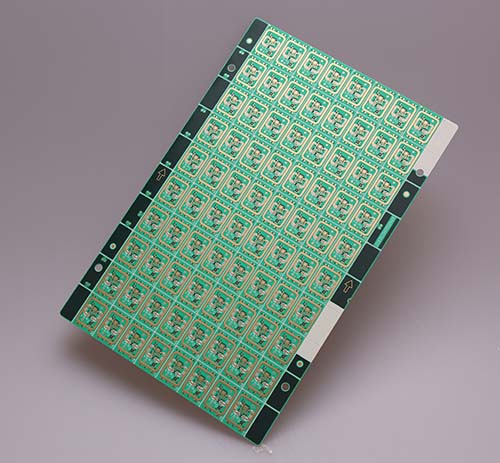
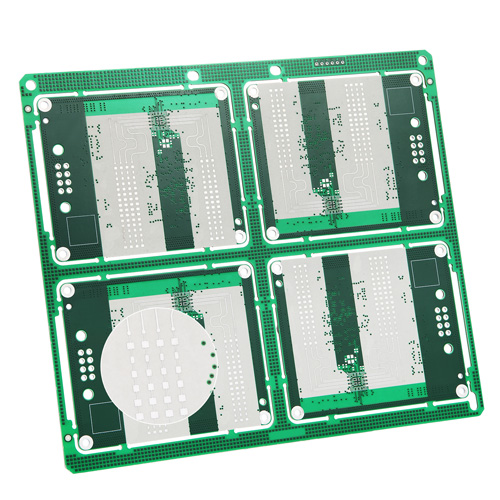
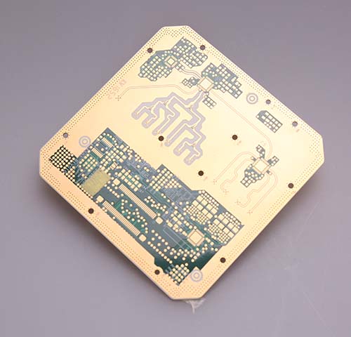
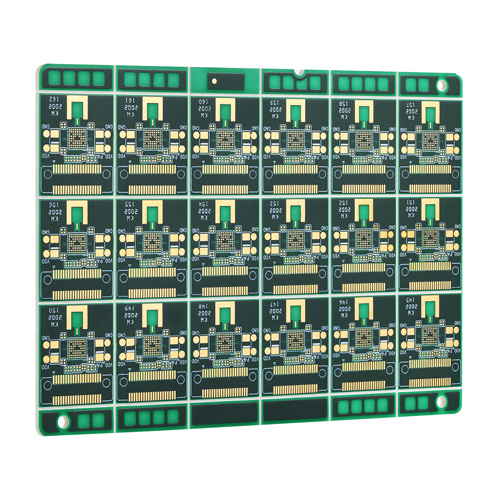
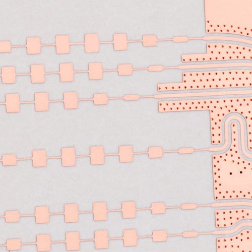
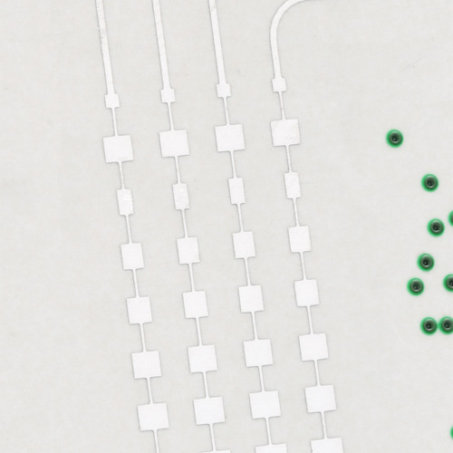
With the widespread application of antennas, ODUs, automotive millimeter wave radars, and satellite communication products, and the gradual increase in radio frequency, higher processing requirements are imposed on PCBs. Kinwong has gained rich processing experience over the years in the application of high-frequency materials, the tightening of RF micro-band line width tolerances, warping control in asymmetric structures, buried copper processes, deep V blind via, POFV, and other special processes.
Kinwong’s technical capabilities are as follows:
Main materials that can be processed: hydrocarbons + ceramic fillers, hydrocarbons + fiberglass fabrics, PPO + fillers, PTFE + ceramic fillers; PTFE + fiberglass fabrics
LDI direct laser imaging, achieving high graphic fidelity, and ensuring simulation effects for customers
Signal line accuracy: ±15μm
Inter-layer alignment: +/-4mil (≤8 layers)
Asymmetric warping <0.5%
Buried via / blind via / micro-via
Mixed compression and buried copper
Main surface finishing: immersion tin, immersion silver, OSP, and ENIG