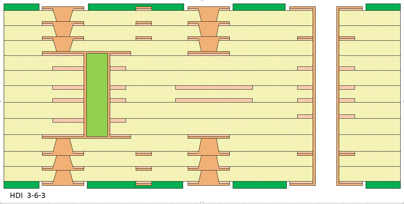
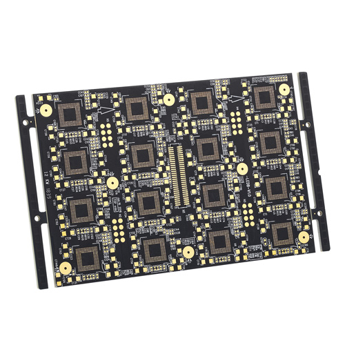
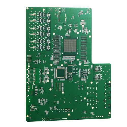
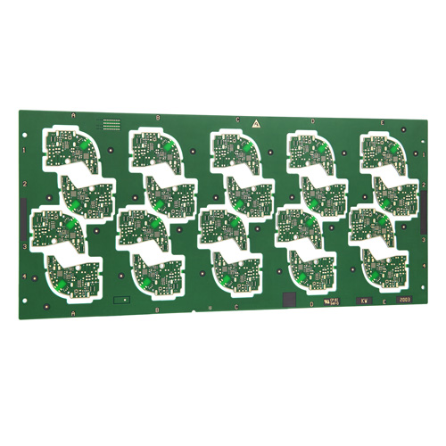
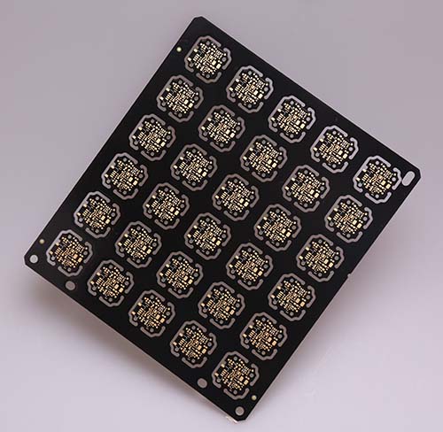
HDI (high density interconnect) PCBs, with micro via holes of ≤0.15mm, connect components in extremely small packages using fine line technology. HDI PCBs have smaller geometric dimensions, and can achieve higher wiring densities. Through control for lower parasitic interference, minimal stubs, the removal of decoupling capacitors, and lower crosstalk, electrical performance is improved greatly. Due to the smaller distance between ground layers, denser distributed capacitance, and smaller RFI and EMI are achieved.
Kinwong’s technical capabilities are as follows:
Increasing line density
Beneficial for the application of advanced packaging technology
Anylayer
mSAP
Advanced equipment
Min. line width / spacing: 30/30μm (mSAP) 40/40μm (tenting)